PRODUCTS

PRODUCTS

CERAMICS
PRODUCT
CERAMICS
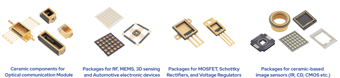
Ceramic Packages and Substrates
RF Materials provides ceramic packages with superior mechanical properties, suitable for small, high density,
and surface mountable applications. Hermetic or vacuum-sealing is typically applied to ensure device quality.
| Applications | Features |
|---|---|
|
Flexible production capability, accepting small-quantity orders to high volume production requirements |
Optical Communications PKG (TOSA/ROSA, BTF, TO) |
| RF Power TR & High Frequency PKG | |
|
Flexible shape capability by strictly controlled green sheet lamination technology |
Various Sensor Package |
| MEMS, SMD Package | |
|
Range of applications from single-layer to multilayer ceramics (Mo/Mn , W etc.) |
Hybrid IC with mixed Power circuit |
| Ceramic Heater | |
|
RFMTL assists in design optimization by providing electrical and thermal simulations |
- |
| - |
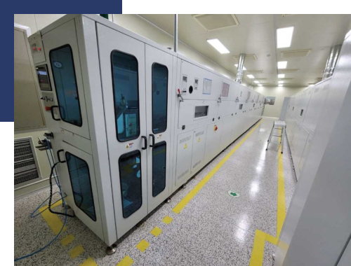
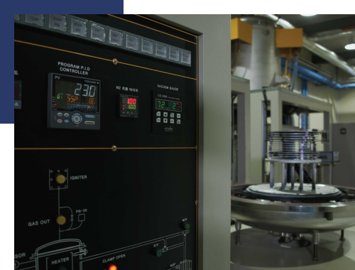
HTCC Multilayer Ceramics Technologies
We are building a ceramic manufacturing platform with a laminate structure based on HTCC. Due to its multilayered
structure, circuit designs can be delivered flexibly through layers and complex structures, e.g. cavity structures, are available.
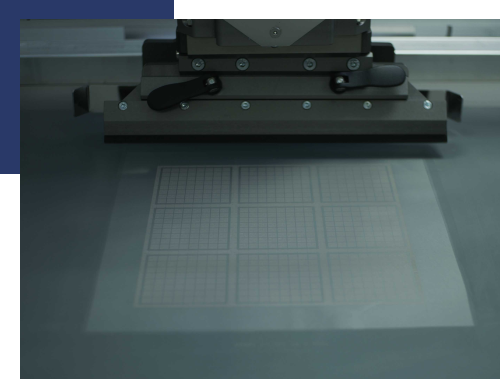
Green Sheet Tape Casting & Sheet Forming
-
Ceramic green sheets are manufactured by the doctor blade method
under strict control - Manufactured thickness range is 0.02~0.5mm (6~12"/sq)
Processing Via and Cavities
-
Processing holes and cavities on ceramic sheets using a punching
pin-die unit -
Drilling & scribing work process on green sheet using CO₂
and IR laser source
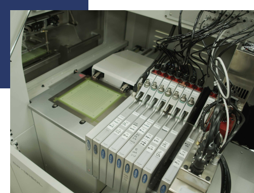
Screen Printing and Lamination
- Printing process for multilayer boards and via-hole filling
- Green sheet lamination process of Multi-layer boards
High Temperature Co-Firing
-
Ceramic firing conditions are produced by Co-debinding & Co-firing in a
humidified hydrogen atmosphere
Ceramic Material Properties and Design Rules
Various bar stacks can meet the needs of diverse customers. We manufacture package and do
packaging in house
Material Properties
| Item | Unit | HTCC | |
|---|---|---|---|
| White | Black | ||
| Material name | - | MHA-94 | MBA-92 |
| Dielectric Constant |
@ 1MHz 10GHz |
9.4 8.8 |
9.8 9.2 |
| Dielectric loss tangent (Tan δ) | @ 1MHz 10GHz |
5x10⁻⁴ 1x10⁻³ |
4x10⁻⁴ 1x10⁻³ |
| Thermal conductivity | W/mK | 26 | 17 |
| TCE | ppm/°C | 7.5 | 7.4 |
| Density | g/cm² | 3.6 | 3.6 |
| Flexural strength | MPa | >350 | >350 |
| Conductor Materials | - | W, Mc | W, Mo |
| Volume Resistivity | Ω.cm | >1012 | >1012 |
| Alumina contents | % | 94 | 92 |
Design Rules for HTCC (EXPOSED SURFACE LAYER)
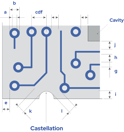
| Location | Spec. | |
|---|---|---|
| a | Via Hole Diameter | ≥150 |
| b | Via Hole Land | ≥400 |
| c | Via Hole Pitch | ≥650 |
| d |
Via Catch Pad to Line
- w/Via from Upper layer - w/o Via from Upper layer |
≥300 ≥200 |
| e | Via Catch Pad to Substrate Edge | ≥650 |
| f | Via Catch Pad to Cavity Edge | ≥650 |
| g | Line Width | ≥150 |
| h | Line Spacing | ≥100 |
| i | Line to Substrate Edge | ≥500 |
| j | Line to Cavity Edge | ≥500 |
| k | Castellation to Line | ≥250 |
| l | Castellation to Via Catch Pad | ≥300 |
HEAD OFFICE231, 215, Gangchon-ro, Danwon-gu, Ansan-si, Gyeonggi-do, Republic of Korea Tel. +82-31-499-2817~8Fax. 031-499-2815
Second factory49, Sandan-ro 20beon-gil, Danwon-gu, Ansan-si, Gyeonggi-do, Republic of Korea 15612. Tel. +82-31-507-0075Fax. 070-8228-0849
COPYRIGHT 2022, RF-Materials CO.,LTD. ALL RIGHTS RESERVED. 관리자